Hi From London England

Re: Hi From London England
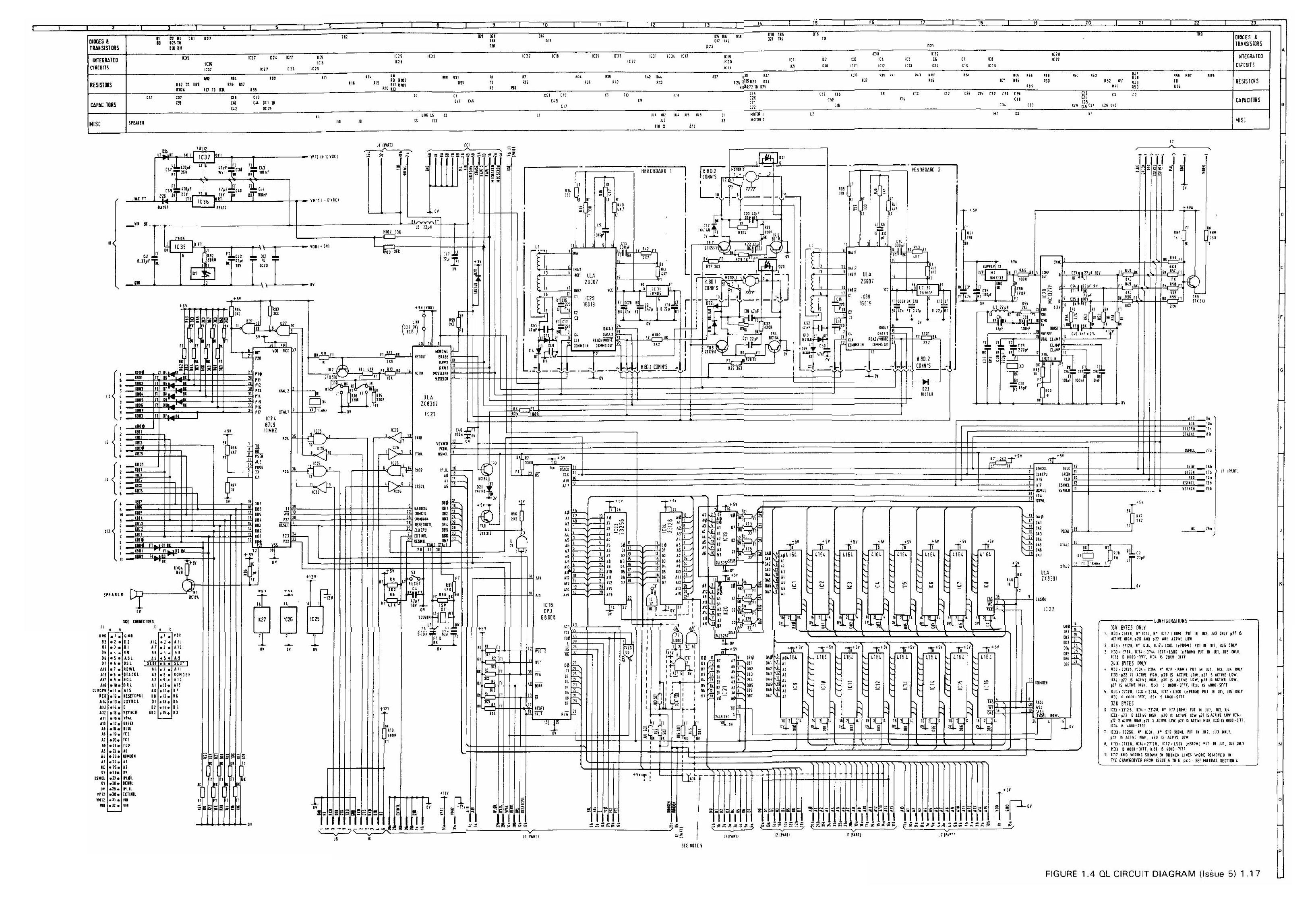
Even then you'd have to move A15 to the top right left hand pin (pin 1), which nominally is at +5v, as for whatever reason Sinclair decided no one would fit a single rom. Only a single gate is needed with a 64K chip, and pin 1 and pin 20 and pin 22 are the ones that need to be displaced to connect up correctly. ROMOEH, needs inverting for use by *OE pin (22) on the 512 eprom, and A15 needs to go to pin 1, but it is currently wired to pin 20. Pin 20 can be either tied to ground, and let the *OE pin on the Eprom do the work of selecting, or tie both these pins together. I am not sure what scheme they used on the Minverva carrier from memory. Fairly sure there is a post about it on here somewhere. You can bundle up TK2 with the ROM image and use up the top quarter of the 512 eprom, so you have a full 64K image.
-
Derek_Stewart

- Font of All Knowledge
- Posts: 4864
- Joined: Mon Dec 20, 2010 11:40 am
- Location: Sunny Runcorn, Cheshire, UK
Re: Hi From London England
Which is the link I referred to on page 4 of this message:
https://www.theqlforum.com/viewtopic.php ... prom#p2740
Regards, Derek

Re: Hi From London England
I've not looked too deeply into this, but the issue 5 circuit diagram says different (http://www.sinclairql.net/srv/QLSchematicIssue5.gif, box bottom right, option 7):Pr0f wrote:Even then you'd have to move A15 to the top right left hand pin (pin 1), which nominally is at +5v, as for whatever reason Sinclair decided no one would fit a single rom. Only a single gate is needed with a 64K chip, and pin 1 and pin 20 and pin 22 are the ones that need to be displaced to connect up correctly. ROMOEH, needs inverting for use by *OE pin (22) on the 512 eprom, and A15 needs to go to pin 1, but it is currently wired to pin 20. Pin 20 can be either tied to ground, and let the *OE pin on the Eprom do the work of selecting, or tie both these pins together. I am not sure what scheme they used on the Minverva carrier from memory. Fairly sure there is a post about it on here somewhere. You can bundle up TK2 with the ROM image and use up the top quarter of the 512 eprom, so you have a full 64K image.
You can fit a single 23256 into the left socket, then set JU2 and JU3 - Voilá, single ROM solution.
Tobias
ʎɐqǝ ɯoɹɟ ǝq oʇ ƃuᴉoƃ ʇou sᴉ pɹɐoqʎǝʞ ʇxǝu ʎɯ 'ɹɐǝp ɥO
Re: Hi From London England
The only problem there is that 23256 is only capable of holding a 32K image, and the other issue is that the original poster has 2 x 27256 chips which are negative going OE and CE, unlike the ROM chips which have been masked programmed to accept a positive going OE and potentially CE as well.tofro wrote:I've not looked too deeply into this, but the issue 5 circuit diagram says different (http://www.sinclairql.net/srv/QLSchematicIssue5.gif, box bottom right, option 7):Pr0f wrote:Even then you'd have to move A15 to the top right left hand pin (pin 1), which nominally is at +5v, as for whatever reason Sinclair decided no one would fit a single rom. Only a single gate is needed with a 64K chip, and pin 1 and pin 20 and pin 22 are the ones that need to be displaced to connect up correctly. ROMOEH, needs inverting for use by *OE pin (22) on the 512 eprom, and A15 needs to go to pin 1, but it is currently wired to pin 20. Pin 20 can be either tied to ground, and let the *OE pin on the Eprom do the work of selecting, or tie both these pins together. I am not sure what scheme they used on the Minverva carrier from memory. Fairly sure there is a post about it on here somewhere. You can bundle up TK2 with the ROM image and use up the top quarter of the 512 eprom, so you have a full 64K image.
You can fit a single 23256 into the left socket, then set JU2 and JU3 - Voilá, single ROM solution.
Tobias

Re: Hi From London England
Yes Derek I was not ignoring your suggestion but it is only now that Pr0f has shown me that putting two 32K EPROMs in is harder than one 64K. It doesn't matter to me if the internal ROM area takes the ROM slot space since I was going to try the Tychie code anyway.Derek_Stewart wrote:Which is the link I referred to on page 4 of this message:
https://www.theqlforum.com/viewtopic.php ... prom#p2740
Like you say Pr0f invert ROMOEH and connect the two enable signals then put A15 on pin 1 for 27512 chip. Simple when you say it quick.
Re: Hi From London England
After jumping through hoops I have decided not to modify the board to fit one 64K EPROM because it just looks too complicated track wise. So I am going to make a daughter board where I can add a transistor to invert the ROMOEH line and just wire all the other lines where I want. It is better to pull the chip enable *E line permanently to zero to avoid any timing issues because the data says it has to be set first before the output enable *G. I shall straddle the daughter board across the two ROM sockets so it picks up lines 1 to 14 on IC33 and 15 to 28 on IC34 so it makes the board bigger and makes things easy to wire. I still don't know if a new ROM is going to fix the QL but the board will give me the ability to program EPROMs with test code if normal code doesn't work. If there is any errors in these thoughts please let me know before I cock it up. 
Re: Hi From London England
Well, you could do worse than looking at the QLSD hardware (http://www.dilwyn.me.uk/qlsd/) schematics.
This uses a 64k EPROM connected to one single ROM socket - It obviously also uses a CPLD for address decoding (which is way too large for your purposes and way too small for soldering at home), but that could be simplified to a GAL, for example. And it doesn't need any mods on the mainboard.
Tobias
This uses a 64k EPROM connected to one single ROM socket - It obviously also uses a CPLD for address decoding (which is way too large for your purposes and way too small for soldering at home), but that could be simplified to a GAL, for example. And it doesn't need any mods on the mainboard.
Tobias
ʎɐqǝ ɯoɹɟ ǝq oʇ ƃuᴉoƃ ʇou sᴉ pɹɐoqʎǝʞ ʇxǝu ʎɯ 'ɹɐǝp ɥO