Page 3 of 12
Re: DIY RAM EXPANSION
Posted: Fri Apr 18, 2014 4:41 pm
by dilwyn
Nasta wrote:tofro wrote:Dave wrote:
What I want to know is.... Who is Dawn?

She's living under my Gold card.
IIRC girlfriend of the guy who worked with Stuart Honeyball and designed both the GC and SGC PCBs, whose name escapes me...
Mike Tomlinson.
Re: DIY RAM EXPANSION
Posted: Sun Apr 20, 2014 7:54 am
by tcat
Hi All,
I have started my PCB design, as it seems a better option to using prototype backplane board.
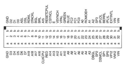
I seem a little bit confused about DIN expansion connector pinnout.
QL Concepts Guide gives such pinout as MALE, I guess I need to put FEMALE in the design, but there is yet another view such as solder side, connector side.
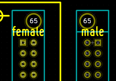
My design software offers these two DIN pinouts, it is top view solder side.
Can anyone help to choose?
Many thanks TCAT

- QL DIN pinout
Re: DIY RAM EXPANSION
Posted: Sun Apr 20, 2014 10:18 am
by tofro
Dave,
according to the document on the Reichelt site, the "a" row is always the bottommost on the connector and the pin row closest to the card edge. Your picture seems to show the non-angled connector pinouts - They are slightly different and have the mounting (screw) between "a" and "b", but closer to the "b" row. The angled ones have it outside (towards card edge) of "a".
Hope this doesn't confuse even more....
Tobias
Re: DIY RAM EXPANSION
Posted: Sun Apr 20, 2014 1:05 pm
by tcat
Tobias,
"A" pins are on the edge, I was afraid so.
Meaning that "A" row contains most of the address and data line pins, this makes it difficult for track routing. To reach address and data pins on the PCB the tracks would have to go between many "B" row pins.
Correct?
Many thanks so far.
TCAT
Re: DIY RAM EXPANSION
Posted: Sun Apr 20, 2014 2:25 pm
by Dave
Hi TCAT,

I have also had this struggle. Mostly because the labels do not match the markings

The square hole is pin 1. That usually means pin one of row A, which is the row closest to the board's edge. In this case, the square hole would go at the bottom/front of the board, nearest the board edge.
However, if you're not working from a schematic, as long as the positioning is correct it really doesn't matter.
Re: DIY RAM EXPANSION
Posted: Mon Apr 21, 2014 5:28 pm
by tcat
Just to double check.
This is what I see when looking inside the QL slot.
From left to righ
"B" row top, GND, D2, D1, D0, ...
"A" row bottom, GND, D3, D4, D5, ...
Correct?
TCAT

- QL expansion connector FRONT view
Re: DIY RAM EXPANSION
Posted: Mon Apr 21, 2014 6:05 pm
by prime
tcat wrote:Just to double check.
This is what I see when looking inside the QL slot.
From left to righ
"B" row top, GND, D2, D1, D0, ...
"A" row bottom, GND, D3, D4, D5, ...
Correct?
TCAT
QL_expansion.jpg
No I think that's what you would see looking into the connector on an expansion card CARD (or from the QL side of the connector. Looking into the slot it would be mirrored left to right do GND and the data lines would be on the RIGHT.
Cheers.
Phill.
Re: DIY RAM EXPANSION
Posted: Mon Apr 21, 2014 7:04 pm
by tcat
Dave, Phill,
Expansion card edge with connector imprint, TOP VIEW, should look like that.
Correct?
Thanks so far.
TCAT

- QL expansion card edge
Re: DIY RAM EXPANSION
Posted: Mon Apr 21, 2014 8:30 pm
by Dave
Yes, the two ground pins 1a and 1b are at the bottom. The three VIN pins are at the top, 32a and 32b, plus 31b.
I made this handy laminate that I use with a dry erase marker when hooking stuff up - great for keeping track...
QL on right, thru-conn on left.

Re: DIY RAM EXPANSION
Posted: Tue Apr 22, 2014 8:36 pm
by tcat
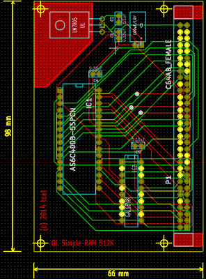
My first ever PCB, 3 vias in grey, unconnected pads in yellow.
I skipped prototype backplane, relying mostly on forum advice, how certain can I be, it will work in the end?
Thank you ALL so far.
TCAT

- ql520 ram pcb